- 您现在的位置:买卖IC网 > Sheet目录3832 > PIC16C924-04/L (Microchip Technology)IC MCU OTP 4KX14 LCD DVR 68PLCC
PIC16C9XX
DS30444E - page 12
1997 Microchip Technology Inc.
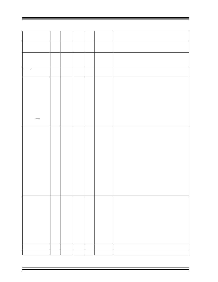
TABLE 3-1: PIC16C9XX PINOUT DESCRIPTION
Pin Name
DIP
Pin#
PLCC
Pin#
TQFP
Pin#
Pin
Type
Buffer
Type
Description
OSC1/CLKIN
22
24
14
I
ST/CMOS
Oscillator crystal input or external clock source input. This
buffer is a Schmitt Trigger input when congured in RC
oscillator mode and a CMOS input otherwise.
OSC2/CLKOUT
23
25
15
O
—
Oscillator crystal output. Connects to crystal or resonator
in crystal oscillator mode. In RC mode, OSC2 pin outputs
CLKOUT which has 1/4 the frequency of OSC1, and
denotes the instruction cycle rate.
MCLR/VPP
1
2
57
I/P
ST
Master clear (reset) input or programming voltage input.
This pin is an active low reset to the device.
PORTA is a bi-directional I/O port. The AN and VREF multi-
plexed functions are used by the PIC16C924 only.
RA0/AN0
4
5
60
I/O
TTL
RA0 can also be Analog input0.
RA1/AN1
5
6
61
I/O
TTL
RA1 can also be Analog input1.
RA2/AN2
7
8
63
I/O
TTL
RA2 can also be Analog input2.
RA3/AN3/VREF
8
9
64
I/O
TTL
RA3 can also be Analog input3 or A/D Voltage Refer-
ence.
RA4/T0CKI
9
10
1
I/O
ST
RA4 can also be the clock input to the Timer0
timer/counter. Output is open drain type.
RA5/AN4/SS
10
11
2
I/O
TTL
RA5 can be the slave select for the synchronous serial
port or Analog input4.
PORTB is a bi-directional I/O port. PORTB can be software
programmed for internal weak pull-ups on all inputs.
RB0/INT
12
13
4
I/O
TTL/ST
RB0 can also be the external interrupt pin. This buffer
is a Schmitt Trigger input when congured as an exter-
nal interrupt.
RB1
11
12
3
I/O
TTL
RB2
3
4
59
I/O
TTL
RB3
2
3
58
I/O
TTL
RB4
64
68
56
I/O
TTL
Interrupt on change pin.
RB5
63
67
55
I/O
TTL
Interrupt on change pin.
RB6
61
65
53
I/O
TTL/ST
Interrupt on change pin. Serial programming clock.
This buffer is a Schmitt Trigger input when used in
serial programming mode.
RB7
62
66
54
I/O
TTL/ST
Interrupt on change pin. Serial programming data.
This buffer is a Schmitt Trigger input when used in
serial programming mode.
PORTC is a bi-directional I/O port.
RC0/T1OSO/T1CKI
24
26
16
I/O
ST
RC0 can also be the Timer1 oscillator output or
Timer1 clock input.
RC1/T1OSI
25
27
17
I/O
ST
RC1 can also be the Timer1 oscillator input.
RC2/CCP1
26
28
18
I/O
ST
RC2 can also be the Capture1 input/Compare1 out-
put/PWM1 output.
RC3/SCK/SCL
13
14
5
I/O
ST
RC3 can also be the synchronous serial clock
input/output for both SPI and I2C modes.
RC4/SDI/SDA
14
15
6
I/O
ST
RC4 can also be the SPI Data In (SPI mode) or data
I/O (I2C mode).
RC5/SDO
15
16
7
I/O
ST
RC5 can also be the SPI Data Out (SPI mode).
C1
16
17
8
P
LCD Voltage Generation.
C2
17
18
9
P
LCD Voltage Generation.
Legend: I = input
O = output
P = power
L = LCD Driver
— = Not used
TTL = TTL input
ST = Schmitt Trigger input
发布紧急采购,3分钟左右您将得到回复。
相关PDF资料
PIC16F767-I/SO
IC PIC MCU FLASH 8KX14 28SOIC
PIC24FJ64GA310-I/PF
MCU 16BIT 64KB FLASH 100TQFP
DSPIC33FJ64GP202-E/MM
IC DSPIC MCU/DSP 64K 28-QFN
PIC16F876A-I/ML
IC MCU FLASH 8KX14 A/D 28QFN
PIC16F876A-I/SO
IC MCU FLASH 8KX14 EE 28SOIC
PIC16F876A-I/SP
IC MCU FLASH 8KX14 EE 28DIP
AT87C51RD2-3CSUM
IC 8051 MCU 64K OTP 40MHZ 40DIP
DSPIC33FJ64MC802-I/SO
IC DSPIC MCU/DSP 64K 28-SOIC
相关代理商/技术参数
PIC16C924-04/PT
功能描述:8位微控制器 -MCU 7KB 176 RAM 52 I/O RoHS:否 制造商:Silicon Labs 核心:8051 处理器系列:C8051F39x 数据总线宽度:8 bit 最大时钟频率:50 MHz 程序存储器大小:16 KB 数据 RAM 大小:1 KB 片上 ADC:Yes 工作电源电压:1.8 V to 3.6 V 工作温度范围:- 40 C to + 105 C 封装 / 箱体:QFN-20 安装风格:SMD/SMT
PIC16C924-04I/L
功能描述:8位微控制器 -MCU 7KB 176 RAM 52 I/O RoHS:否 制造商:Silicon Labs 核心:8051 处理器系列:C8051F39x 数据总线宽度:8 bit 最大时钟频率:50 MHz 程序存储器大小:16 KB 数据 RAM 大小:1 KB 片上 ADC:Yes 工作电源电压:1.8 V to 3.6 V 工作温度范围:- 40 C to + 105 C 封装 / 箱体:QFN-20 安装风格:SMD/SMT
PIC16C924-04I/PT
功能描述:8位微控制器 -MCU 7KB 176 RAM 52 I/O RoHS:否 制造商:Silicon Labs 核心:8051 处理器系列:C8051F39x 数据总线宽度:8 bit 最大时钟频率:50 MHz 程序存储器大小:16 KB 数据 RAM 大小:1 KB 片上 ADC:Yes 工作电源电压:1.8 V to 3.6 V 工作温度范围:- 40 C to + 105 C 封装 / 箱体:QFN-20 安装风格:SMD/SMT
PIC16C924-08/L
功能描述:8位微控制器 -MCU 7KB 176 RAM 52 I/O RoHS:否 制造商:Silicon Labs 核心:8051 处理器系列:C8051F39x 数据总线宽度:8 bit 最大时钟频率:50 MHz 程序存储器大小:16 KB 数据 RAM 大小:1 KB 片上 ADC:Yes 工作电源电压:1.8 V to 3.6 V 工作温度范围:- 40 C to + 105 C 封装 / 箱体:QFN-20 安装风格:SMD/SMT
PIC16C924-08/PT
功能描述:8位微控制器 -MCU 7KB 176 RAM 52 I/O RoHS:否 制造商:Silicon Labs 核心:8051 处理器系列:C8051F39x 数据总线宽度:8 bit 最大时钟频率:50 MHz 程序存储器大小:16 KB 数据 RAM 大小:1 KB 片上 ADC:Yes 工作电源电压:1.8 V to 3.6 V 工作温度范围:- 40 C to + 105 C 封装 / 箱体:QFN-20 安装风格:SMD/SMT
PIC16C924-08I/L
功能描述:8位微控制器 -MCU 7KB 176 RAM 52 I/O RoHS:否 制造商:Silicon Labs 核心:8051 处理器系列:C8051F39x 数据总线宽度:8 bit 最大时钟频率:50 MHz 程序存储器大小:16 KB 数据 RAM 大小:1 KB 片上 ADC:Yes 工作电源电压:1.8 V to 3.6 V 工作温度范围:- 40 C to + 105 C 封装 / 箱体:QFN-20 安装风格:SMD/SMT
PIC16C924-08I/PT
功能描述:8位微控制器 -MCU 7KB 176 RAM 52 I/O RoHS:否 制造商:Silicon Labs 核心:8051 处理器系列:C8051F39x 数据总线宽度:8 bit 最大时钟频率:50 MHz 程序存储器大小:16 KB 数据 RAM 大小:1 KB 片上 ADC:Yes 工作电源电压:1.8 V to 3.6 V 工作温度范围:- 40 C to + 105 C 封装 / 箱体:QFN-20 安装风格:SMD/SMT
PIC16C924CL
制造商:MICROCHIP 功能描述:New